Differential ADC simulation
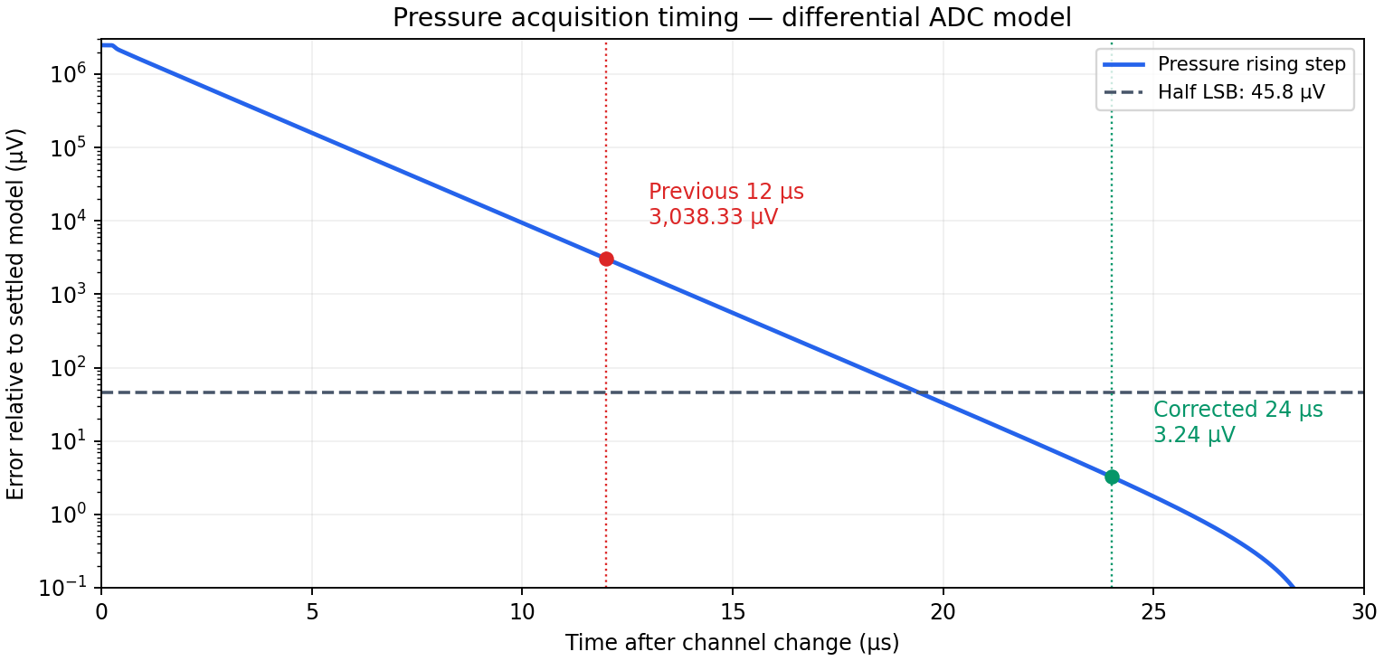
The high-capacitance pressure rising-step case exposed an insufficient 12 µs acquisition wait. The firmware now uses 24 µs for pressure and retains 6 µs for acoustic channels. All five extended native runs complete and meet the half-LSB settling criterion at those windows.
| Case | Wait, µs | Last half-LSB crossing, µs | Sample residual, µV | Modeled DC error, µV |
|---|---|---|---|---|
| dynamic-up | 6 | 5.262 | 18.290 | 122.890 |
| dynamic-down | 6 | 5.262 | -18.290 | 175.143 |
| pressure-up | 24 | 19.420 | -3.244 | 105.926 |
| pressure-down | 24 | 10.675 | 0.001 | 21362.533 |
| dynamic-resistance-stress | 6 | 5.726 | 32.571 | 121.182 |
With the longer settled reference, the old12 µs pressure-up residual is -3038.33 µV;24 µs gives -3.24 µV. The full scan allocates144 µs to settling plus21 µs conversion and21 µs serial clocks, leaving64 µs of a250 µs frame for other overhead. That arithmetic still requires physical timing qualification.
Exact scope
Both OPA320 paths and the OPA4323 bank buffer use the retained original TI equations. The actual22 Ω/1 nF positive and negative buckets and canonical pin mappings are checked. Each input sees a200 Ω/31 pF continuous acquisition equivalent. The native80 µs endpoint, finite samples, diagnostics and completion marker are required before evaluating results. Full traces are retained compressed.
The mux1–2 kΩ/80–160 pF/40–80 pF values are engineering stress assumptions. A10 kΩ source and a full0→2.5 V transition deliberately combine a high source impedance with a maximum step. Supply3.3 V and midpoint1.25 V remain ideal boundaries. The SAR converter is not modeled transistor by transistor; switching charge, reference pulses, temperature, EMI and board/cable parasitics remain separate checks.
The modeled zero-voltage input bottoms near21.39 mV because amplifier outputs cannot reach an ideal ground rail. This is a DC endpoint issue, separate from settling. Pressure calibration must capture the assembled channel’s unloaded endpoint and loaded response. A normalized voltage is not calibrated force.
Original12 µs cases are retained as diagnostic evidence under the scratch review; the published runner binds its waiting times to the current firmware contract. It also supports a separately labeled bias-ramp sensitivity run.
Reproduce: python3 hardware/glove-v4/verification/differential-adc/run.py --work /tmp/glove-adc-check. Requires NumPy and the recorded ngspice42/XSPICE model environment.